ECOLE POLYTECHNIQUE DE LOUVAIN
INTRISIC PHONON-LIMITED CARRIER MOBILITY
The link of the jupiter notebooks that where created to compute the following equations is hosted in this link https://github.com/ndejaegher/Solar_cell
Theorical background
The carrier drift mobility of the semiconductor will be compute with this equation:
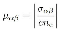
with e the elementary charge, the charge carrier density entering the mobility tensor of the electron n_c and the conductivity tensor σ_αβ.
The following development used to compute the carrier mobility is described in the paper published by S. Poncé et al. [44]
The conductivity tensor defined as:

where:
• e = 1.602119 C
• The macroscopic average of current density J(r) can be expressed as a function of the external electric field E:
• fnk is the out-of-equilibrium occupation of the state nk.
• ∂Eβ fnk is a short-hand notation of the expression (∂f_nk/∂E_β)|E=0 .
• Vuc is the volume of the primitive unit cell.
• Ω_BZ is the volume of the first Brillouin zone.
• v_nk^α = ℏ^{−1} ∂ε_{nk}/∂k_α is the carrier velocity.
The charge carrier density entering the mobility tensor of the electron, n_c = n_e is defined as:

with:
• CB being the set of all conduction bands. In the case of the hole mobility, n_c = n_h, the sum will be over all n into the set of all valence band VB.
• f^0_nk (εF, T) = 1/ {exp [(ε_nk − ε_F) / (k_BT)] + 1} wich is related to the Fermi-Dirac distribution for energy occupation states when no electric field is applied on the semi-conductor.
Hypothesis
In the case of this application, some assumptions are done. In order to compute the conductivity tensor, the relation ∂Eβ fnk wich can be obtained by solving the Boltzmann transport equation (BTE), is approximated with the self-energy relaxation time approximation (SERTA) to obtain:

where τ_nk is the scattering rate which is defined as

But at first instance, according to [45], a good approximation of the scattering rate for the electron carrier mobility of the MAPI perovskite in thin film would be in a magnitude of 10^{−15}s = 1fs as shown in Fig.36.

Figure 36: "Comparison of scattering times vs temperature for 2 MAPbI3(Cl) perovskite films (blue - sample with 27 cm2V −1 s−1; red - sample with 22 cm2V −1 s−1) with different OD at 480 nm"[45]
A second approximation is to consider that f^0_nk(ϵ_f , 0) = 0.
In order to simplify the python script, the volume of the primitive unit cell and the volume of the first Brillouin zone are simplified in the numerator and in the denominator. That leads to a condensed carrier drift mobility expression:

The reduced effective mass (µ) of the mapi pervoskite measured at orthorhombic phase is equal to 0.104 ± 0.003 me [46]. In order to obtain the electron (me*) and hole (mH∗) effective masses, one uses the theoretical results obtained calculating the Wannier Interpolation of the SS-GW Band Structures 34 in order to weight the theoretical results into the experimental data. The Wannier interpolation of all the DFT and GW band structures is performed using the Wannier90 code which is explained in [47]. As a result, the isotropic electron effective mass (m∗ e ) = 0.203 × me and the isotropic hole effective mass (m∗ h ) = 0.214 × me [48].
A better approximation is made using the effective mass. They are the followings: The mapi has a electron effective mass m_e_eff = [0.62, 0.62, 0.09] and a hole effective mass m_h_eff = [-0.67, -0.67, -0.33] [49]. The Silicon has a longitudinal effective electron mass m_e,l* = [0, 0, 0.92] × me and a transversal effective electron mass m_e,l* = [0.19, 0.19, 0] × me [50]. According to holes, the light holes m_LH = 0.16 (band index=1) and the heavy holes m_HH = 0.25 (band indices 2 and 3)[51]
The first Brillouin zone is needed to compute the carrier drift mobility. The key vectors and the following images are extracted from materials cloud [52]


Figure 37: First Brillouin zone of the CH3NH3P bI3 in orthorhombic phase
Figure 38: First Brillouin zone of the silicon in tetragonal phase
Results
The first curve obtained is the orthorhombic electron carrier mobility in function of the temperature for a constant scattering. From the results for the mobility in this article [53], Two τ are chosen to fit the experimental data at 80K and at 300K. Thereby, τ = 0.86fs and τ = 0.31fs are respectively found. This gives the followings curves in Figure 39

Figure 39: Orthorhombic electron carrier mobility in function of the temperature with constant scattering rate τ = 0.86fs (green) and τ = 0.31fs (magenta). Dot are experimental data obtained in [53].
Comparing it with results obtained in [54], it observed that the SERTA calculation with constant scattering rate keeps quite small values of mobility when the temperature are small. The same observation is made when increasing the τ , then mobility does not decrease sufficiently and the mobility keeps being high. In this case the goal of the project is to study the material at room temperature. This is why the curve obtained for 300k in Figure 39 is the most relevant.

Figure 40: Charge-carrier mobility of MAP bI3 as a function of temperature, where the blue and red circles represent the experimental data of thin film and single crystal, respectively. Each data point was measured repeatedly three times, from which the error bar was determined by the standard deviation. The orange line represents the ab initio BTE calculation of intrinsic phonon-limited mobility where all the phonon modes are included, while the green line represents the BTE calculation including grainboundary scattering with crystal size g = 100 nm.[54]
Note that taking in account the fact that the previous calculations were made in orthorhombic phase. In fact, a better approximation can be made using the tetragonal phase which is the phase of the MAPI between 162.2K and 327.4K. The plot mobility of the holes calculated using the same scattering rate as the one used for the orthorhombic electrons carrier mobility is found in Figure 41. Similar slopes are found comparing with Figure 39. Globally, the curve of the holes’ mobility is translated to the left. In order to obtain a smaller mobility for the holes. As well as illustrated in Figure 42.

Figure 41: Orthorhombic holes carrier mobility in function of the temperature with constant scattering rate τ = 0.86fs (green) and τ = 0.31fs (magenta). Dots are experimental data obtained in [53].

Figure 42: DFT simulations of the temperature dependence of the electron and hole mobilities.[55]
Using the same calculation with the silicon, the following mobilities are obtained


Figure 43: electrons and holes carrier mobility in function of the temperature with constant scattering rate τ = 0.003fs. Dots are experimental data obtained in [56]
In order to go further, these are elements that could have been improved. First, to obtain a good value of the hole mobility for silicium, the energies of the heavy holes and light holes must be computed as in [57] E(k)=Ak^2±B^2k^4+C^2(kx^2ky^2+ky^2kz^2+kz^2kx^2)]^{1/2} where A, B and C are inverse band parameters .
Then, the scattering rates where constant in our simulations. Using SERTA approximation and the relation for scattering rate would give mobilites more accurates for large range of temperature.
In conclusion, according to calculation and the comparison of Silicon, mapi and other materials at room temperature in [44]. The mobility of the Silicon still better than mapi.